Why GPUs are the New Kings of Cache. Explained.
It wasn't that far back that if you wanted a processor with tons of cache buried inside it, then CPUs were the obvious choice. Now, even budget-level GPUs come packed with more internal memory than a high-end CPU from barely a few years ago.
So, what changed? Why did graphics chips suddenly need more cache than a generalized, central processor? Is the specialized memory different between the two and will we see GPUs in the future with gigabytes of cache?
To answer these questions, we need to peek under the hood of the latest chips and observe the changes over the years.
TL;DR: Why GPUs have gained so much cache
Low-level data caches have grown in size because GPUs are now utilized in a variety of applications, not just graphics. To improve their capabilities in general-purpose computing, graphics chips require larger caches. This ensures that no math core is left idle, waiting for data.
Last-level caches have expanded considerably to offset the fact that DRAM performance hasn't kept pace with the advancements in processor performance. Substantial L2 or L3 caches reduce cache misses. This also prevents cores from being idle and minimizes the need for very wide memory buses.
Additionally, advances in rendering techniques, especially ray tracing, place immense demands on a GPU's cache hierarchy. Large last-level caches are vital to ensure that game performance, when using these techniques, remains playable.
Cache course 101
To address the topic of cache in full, we must first understand what cache is and its significance. All processors require memory to store the numbers they crunch and the resulting calculations. They also need specific instructions on tasks, such as which calculations to perform. These instructions are stored and conveyed numerically.
This memory is commonly referred to as RAM (Random Access Memory). Every electronic device with a processor is equipped with RAM. For several decades, PCs have employed DRAM (the "D" stands for dynamic) as temporary storage for data, with disk drives serving as long-term storage.
Since its invention, DRAM has seen tremendous improvements, becoming exponentially faster over time. The same applies to data storage, with once dominant but slow hard drives being replaced by swift solid-state storage (SSD). However, despite these advancements, both types of memory are still desperately slow compared to how quickly a basic processor can carry out a single calculation.
Even a set of DDR5-8200 isn't fast enough
While a chip can add two numbers in a few nanoseconds, retrieving those values or storing the result can take hundreds to thousands of nanoseconds – even with the fastest available RAM. If there was no way to get around this, then PCs wouldn't be that much better than those from the 1970s, even though they have much higher clock speeds.
Thankfully, there's SRAM (Static RAM) to bridge this gap. SRAM is made from the same transistors as those in the processors performing the calculations. This means SRAM can be integrated directly into the chipand operate at the chip's speed. Its proximity to the logic units shortens data retrieval or storage times to tens of nanoseconds.
The downside to this is that the arrangement of transistors needed for even a single memory bit, along with other necessary circuitry, occupies a considerable amount of space. Using current manufacturing techniques, 64 MB of SRAM would be roughly equivalent in size to 2 GB of DRAM.
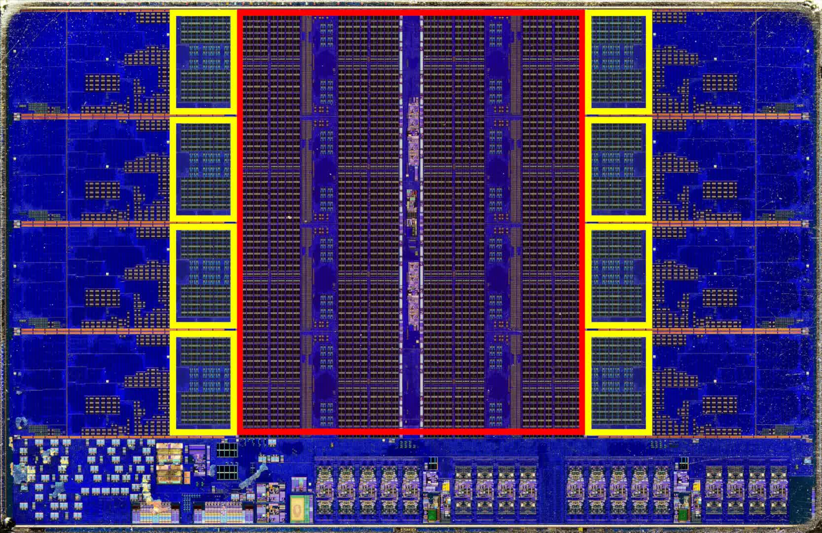
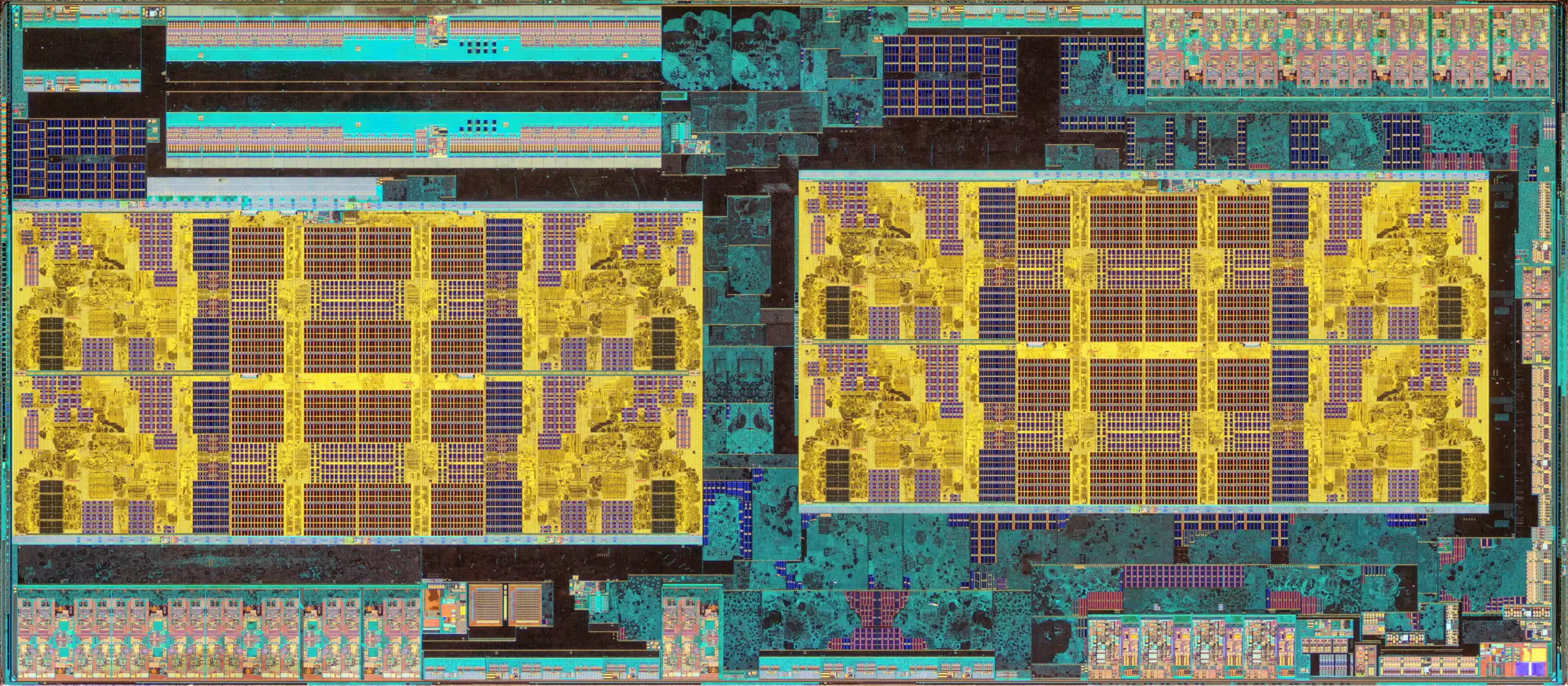
Most of this AMD Zen 4 chiplet is cache (red + yellow boxes). Credit: Fritzchen Fritz
That's why contemporary processors incorporate various SRAM blocks – some minuscule, containing only a few bits, while others hold several MBs. These larger blocks bypass the slowness of DRAM, significantly boosting chip performance.
These memory types go by various names, based on their usage, but the most prevalent is known as "cache." And this is where the discussion becomes a tad more complicated.
All hail the hierarchy
The logic units inside a processor's cores typically work on small pieces of data. The instructions they receive and the numbers they process are rarely larger than 64-bits. Consequently, the tiniest blocks of SRAM, which store these values, are similarly sized and are termed "registers."
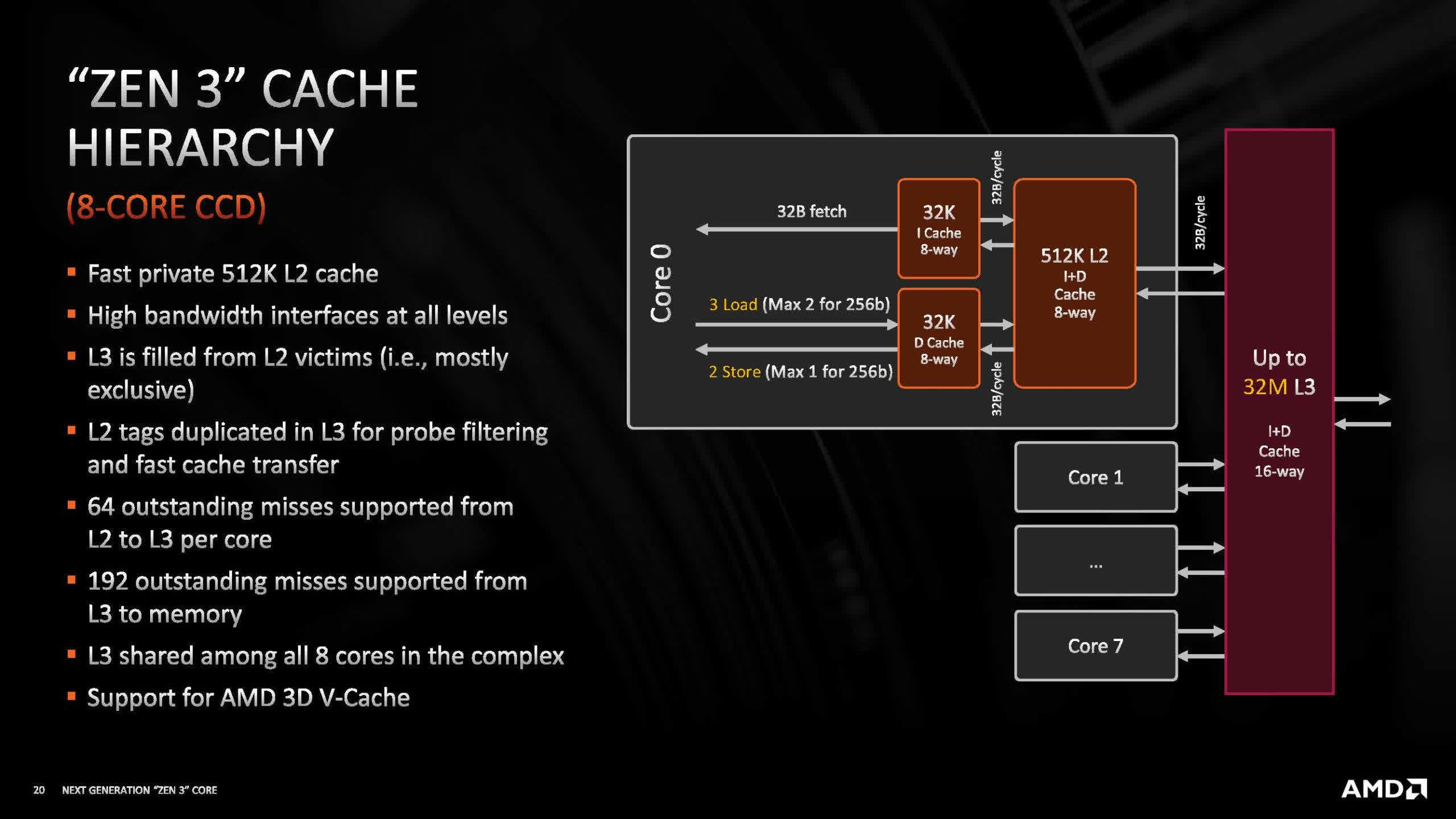
To ensure that these units don't stall, awaiting the next set of commands or data, chips typically prefetch this information and retain frequently issued ones. This data is housed in two distinct SRAM sets, typically referred to as the Level 1 Instruction and Level 1 Data caches. As the names imply, each has a specific type of data it holds. Despite their importance, they're not expansive. For instance, AMD's recent desktop processors allocate 32 kB for each.
Though not very big, these caches are ample enough to hold a significant amount of commands and data, ensuring cores aren't idling. However, to maintain this flow of data, caches must be continuously supplied. When a core requires a specific value not present in a Level 1 cache (L1), the L2 cache becomes crucial.
The L2 cache is a much larger block, storing a diverse range of data. Remember, a single core has multiple logic unit lines. Without the L2, L1 caches would quickly be overwhelmed. Modern processors have multiple cores, prompting the introduction of another cache layer that services all cores: the Level 3 (L3) cache. It's even more expansive, spanning several MBs. Historically, some CPUs even featured a fourth level.
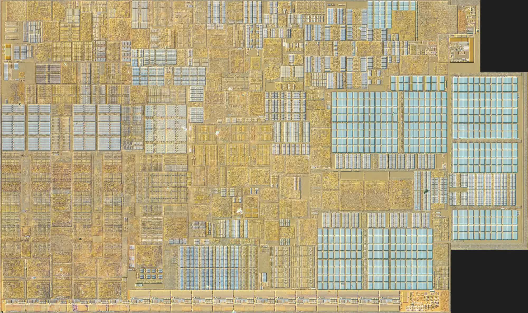
Credit: Fritzchen Fritz
The above image is that of a single P-core from one of Intel's Raptor Lake CPUs. The various grids in pale blue, dotted about the structure, are a mixture of registers and various caches. You can see a more detailed breakdown of each section on this website. However, in essence, the L1 caches are centrally located in the core, while the L2 dominates the right-hand portion.
The last level of cache in processors often acts as the first port of call for any data coming from the system's DRAM, before it gets transferred onward, but that's not always the case. This is the part about cache that tends to get very complex, but it's also crucial to understanding why CPUs and GPUs have very different cache arrangements.
The way that the entire system of SRAM block gets used is known as the cache hierarchyof the chip and it varies enormously, depending on factors such as the age of the architecture and what sector the chip is targeted toward. But for a CPU, there are some aspects that are always the same, one of which is the hierarchy's coherence.
Data in a cache may be replicated from the system's DRAM. If a core modifies it, it's imperative that the DRAM version is concurrently updated. As a result, CPU cache structures possess mechanisms to ensure data accuracy and timely updates. This intricate design adds to the complexity, and in the realm of processors, complexity translates to transistors and subsequently, space.
This is why the first few levels of cache aren't very big – not just because SRAM is pretty spacious, but due to all of the additional systems required to keep it coherent. However, not every processor needs this, and there's one very specific type that generally eschews it altogether.
Cores over cache, the GPU way
Today's graphics chip, in terms of how their internals are arranged and functionality, took form in 2007. This is when both Nvidia and ATI released their unified shader GPUs, but for the latter, the real change took place 5 years later.
In 2012, AMD (who by then had acquired ATI) unveiled their Graphics Core Next (GCN) architecture. This design remains in use today, though it has undergone significant modifications and has evolved into forms like RDNA and CDNA. We'll reference GCN to elucidate the cache differences between CPUs and GPUs, as it presents a clear example.
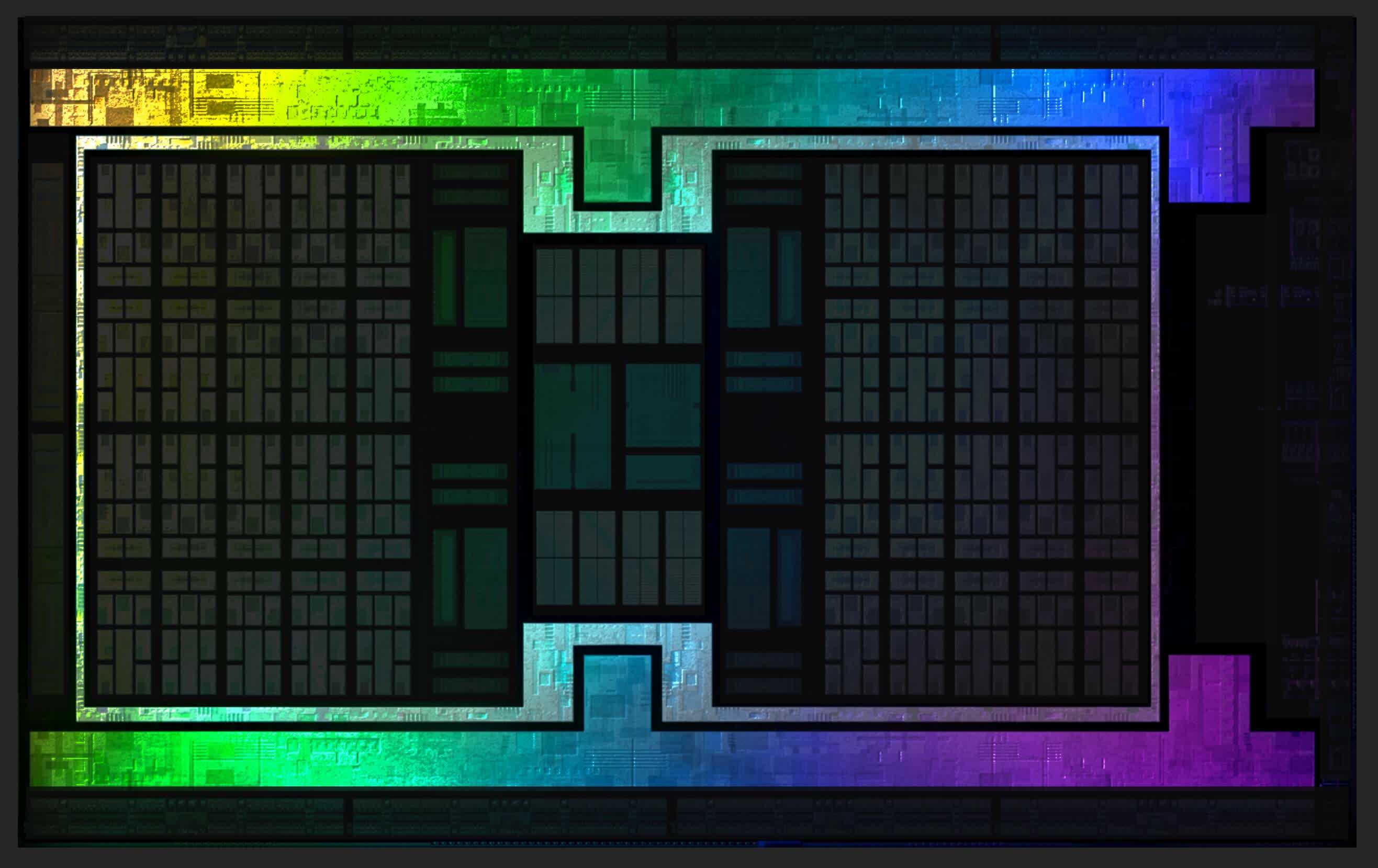
Credit: Fritzchen Fritz
Jumping to 2017, let's contrast AMD's Ryzen 7 1800X CPU (above) with the Radeon RX Vega 64 GPU. The former houses 8 cores, with each core containing 8 pipelines. Four of these pipelines handle standard mathematical operations, two specialize in extensive floating-point calculations, and the last two oversee data management. Its cache hierarchy is structured as follows: 64 kB L1 instruction, 32 kB L1 data, 512 kB L2, and 16 MB L3.
The Vega 64 GPU features 4 processing blocks. Each of these blocks contains 64 pipelines, more commonly termed Compute Units (CUs). Furthermore, each CU accommodates four sets of 16 logic units. Every CU possesses 16 kB of L1 data cache and 64 kB of scratchpad memory, essentially functioning as cache sans the coherency mechanisms (AMD labels this as the Local Data Share).
Additionally, there are two more caches (16 kB L1 instruction and 32 kB L1 data) that cater to groups of four CUs. The Vega GPU also boasts 4 MB of L2 cache, positioned in two strips, one at the base and the other near the top of the illustrated image below.
Credit: Fritzchen Fritz
This specific graphics processor is double the size of the Ryzen chip in terms of die area. However, its cache occupies a remarkably smaller space than that in the CPU. Why does this GPU maintain a minimal cache, especially concerning the L2 segment, in comparison to the CPU?
Given its significantly higher number of 'cores' compared to the Ryzen chip, one might anticipate that with a total of 4096 math units, a substantial cache would be imperative to maintain a steady data supply. However, CPU and GPU workloads differ fundamentally.
While the Ryzen chip can manage up to 16 threads simultaneously and process 16 distinct commands, the Vega processor might handle a larger number of threads, but its CUs typically execute identical instructions.
Moreover, the math units within each CU synchronously perform identical computations during a cycle. This uniformity classifies them as SIMT (single instruction, multiple threads) devices. GPUs operate sequentially, seldom deviating into alternative processing routes.
To draw a parallel, a CPU processes a diverse range of instructions while ensuring data coherence. On the contrary, a GPU repetitively executes similar tasks, eliminating the need for data coherence and constantly restarting its operations.
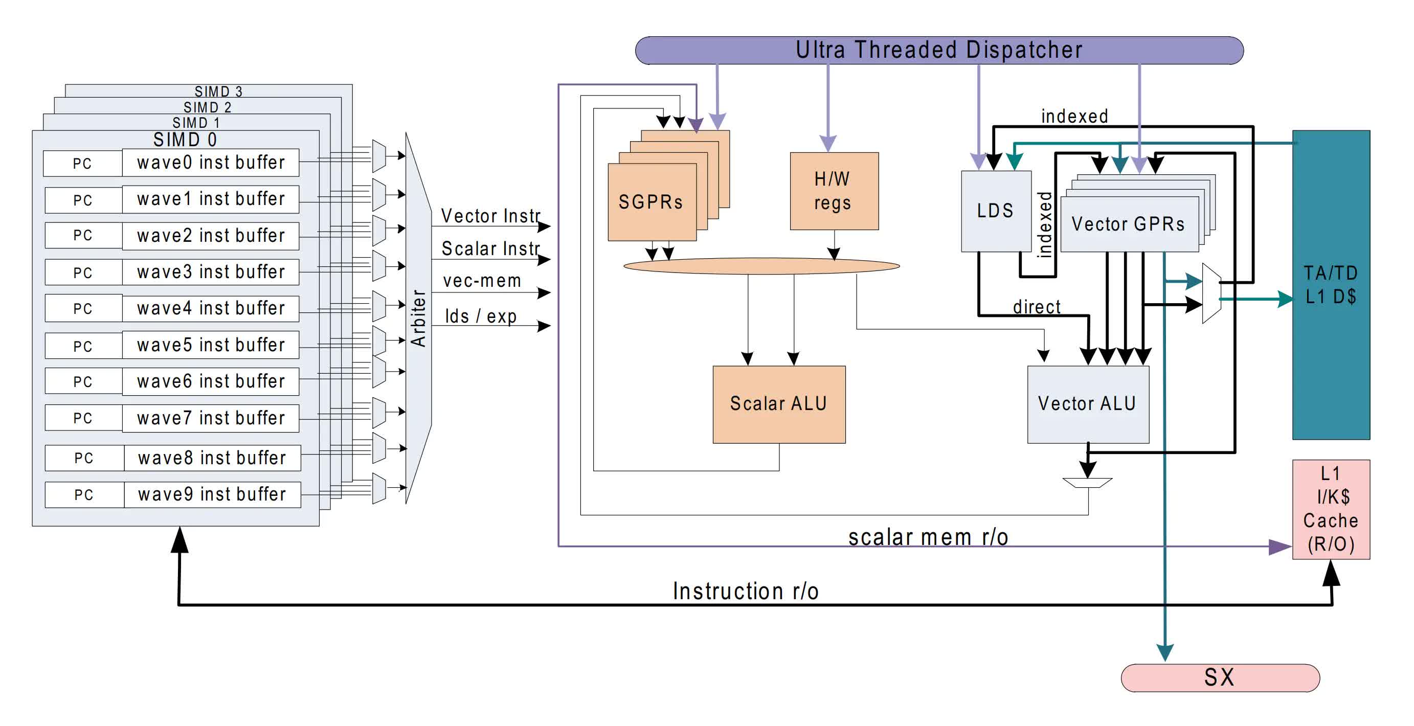
The internal structure of a GCN Compute Unit. Simple, yes?
Because the task of rendering 3D graphics consists largely of repetitive mathematical operations, a GPU doesn't need to be as complex as a CPU. Instead, GPUs are designed to be massively parallel, processing thousands of data points concurrently. This is why they have smaller caches but far more cores, compared to a central processor.
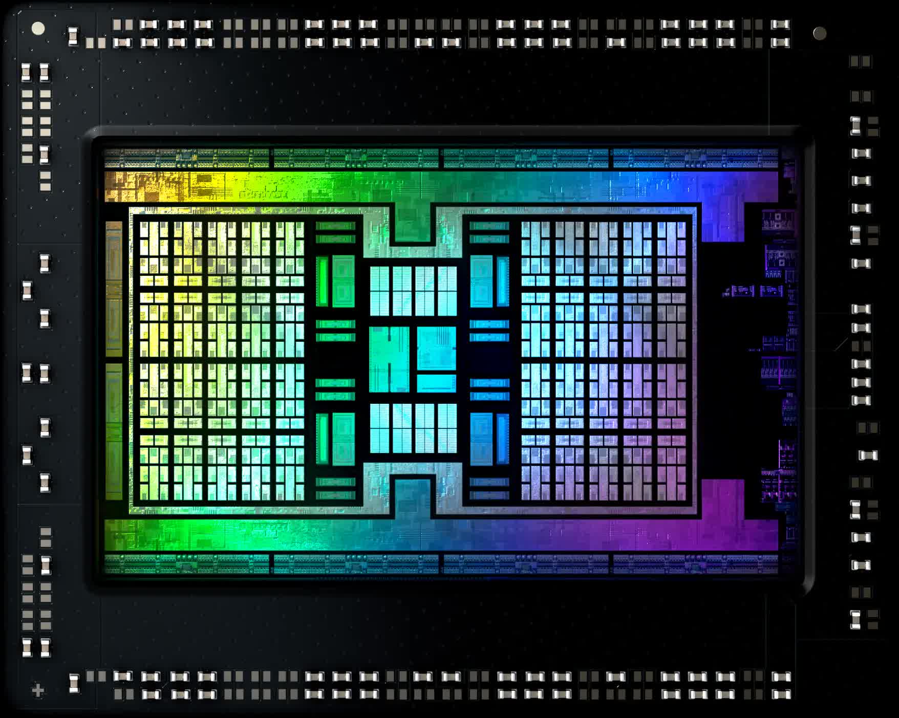
However, if that's the case, why do AMD and Nvidia's latest graphics cards have enormous amounts of cache, even budget models? The Radeon RX 7600 only has 2 MB of L2, but it also sports 32 MB of L3; Nvidia's GeForce RTX 4060 doesn't have L3, but it does come with 24 MB of L2.
And when it comes to their halo products, the numbers are gigantic – the GeForce RTX 4090 boasts 72 MB of L2 and AMD's Navi 21 chip (below) in the Radeon RX 6800 / 6900 cards wades in with 128 MB of L3!
There's quite a bit to unpack here – for example, why did AMD keep the caches so small for so long, but then suddenly boost them in size and throw in a massive amount of L3 for good measure?
Why did Nvidia increase the L1 sizes so much, but keep the L2 relatively small, only to copy AMD and go L2 cache crazy?
That Gin GPU isn't just graphics anymore
There are many reasons for this transformation, but for Nvidia, the shift was driven by changes in how its GPUs were being utilized. Although they are called Graphics Processing Units, these chips were crafted to do much more than merely display impressive images on screens.
While the vast majority of GPUs excel in this function, these chips have ventured beyond the confines of rendering. They now handle mathematical loads in data processing and scientific algorithms across a spectrum of disciplines, including engineering, physics, chemistry, biology, medicine, economics, and geography. The reason? Because they're exceptionally good at doing the same calculation on thousands of data points, all at the same time.
Though CPUs can also perform this function, for certain tasks, a single GPU can be as efficient as multiple central processors. With Nvidia's GPUs evolving to be more general-purpose, both the quantity of logic units within the chip and their operational speeds have witnessed exponential growth.
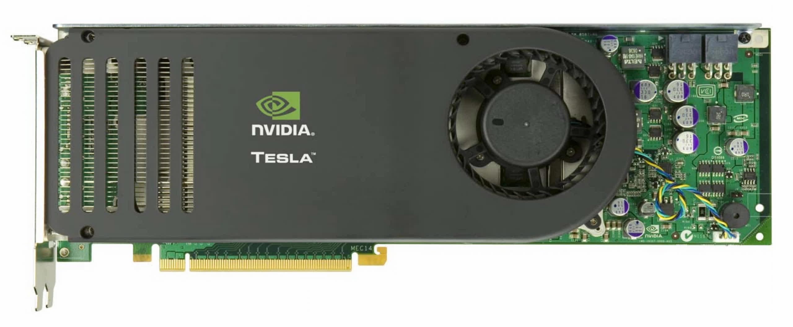
Nvidia's first 'graphics' card for serious general-purpose computing – the Tesla C870 from 2007
Nvidia's debut into serious general-purpose computing was marked by the Tesla C870 in 2007. The architecture of this card, with merely two levels in its cache hierarchy (one could technically argue for 2.5, but let's sidestep that debate), ensured the L1 caches were expansive enough to continually supply data to all the units. This was bolstered by ever-faster VRAM. The L2 cache grew in size, too, though nothing like what we're seeing now.
Nvidia's first couple of unified shader GPUs got by with just 16 kB of L1 data (and a tiny amount for instructions and other values), but this jumped to 64 kB within a couple of years. For the past two architectures, GeForce chips have sported 128 kB of L1 and its server-grade processors sport even more.
The L1 cache in those first chips only had to serve 10 logic units (8 general purpose + 2 special function). By the time the Pascal architecture appeared (roughly the same era as AMD's RX Vega 64), the cache had grown to 96 kB for over 150 logic units.
This cache gets its data from the L2, of course, and as the number of clusters of those units increased with each generation, so too did the amount of L2 cache. However, since 2012, the amount of L2 per logic cluster (better known as a Streaming Multiprocessor, SM) has remained relatively the same – in the order of 70 to 130 MB. The exception is, of course, the latest Ada Lovelace architecture, and we'll come back to this one in a moment.
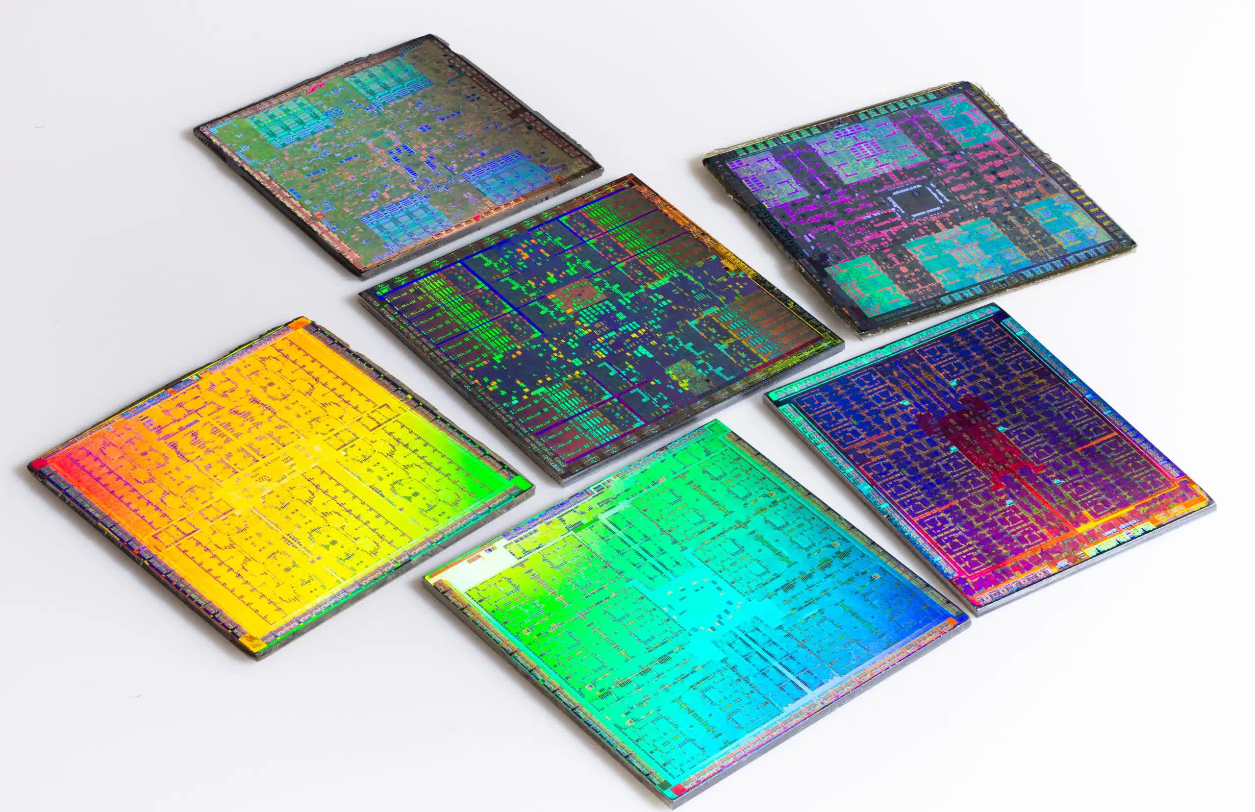
Nvidia's biggest GPUs, 2006 to 2016. Credit: Fritzchen Fritz
For many years, AMD's focus was heavily centered on its CPUs, with the graphics department being relatively small – in terms of staffing and budget. As a fundamental design, though, GCN worked really well, finding a home in PCs, consoles, laptops, workstations, and servers.
While perhaps not always the fastest GPU one could buy, AMD's graphics processors were more than good enough and the cache structure of these chips seemingly didn't need a serious update. But while CPUs and GPUs were growing in leaps and bounds, there was another piece of the puzzle that was proving far harder to improve.
DRAM drags its heels
The successor to GCN was the 2019 RDNA architecture, for which AMD rejigged everything so that their new GPUs used three levels of cache, while still keeping them relatively small. Then, for its follow-up RDNA 2 design, AMD leveraged its expertise in CPU cache engineering to shoehorn a fourth level of cache into the die – one that was vastly larger than anything seen in a GPU prior to that point.
But why make such a change, especially when these chips were primarily geared for gaming and the GCN caches had seen minimal modifications over the years?
The reasons are straightforward:
- Chip Size and Complexity:While incorporating more cache levels does complicate the chip design, it prevents the chips from becoming excessively large. A smaller chip means more units can be extracted from a single silicon wafer, making them more cost-effective to produce.

- Memory Speed vs. Processor Speed:Processor speeds have been on a consistent rise over the years, but DRAM hasn't matched that pace. For instance, in the Radeon RX Vega 64, AMD utilized High Bandwidth Memory (HBM) to enhance the data transfer rate between the VRAM and GPU. These modules, displayed above to the left of the main GPU die, are essentially multiple DRAM dies stacked together, facilitating more data to be read or written per cycle. However, HBM is notably expensive. Ideally, graphics cards would have ample memory, numerous buses, all operating at high speeds. But due to DRAM's construction, its performance couldn't be escalated to match that of a CPU or GPU.
When data necessary for a computation isn't present in the caches (what's usually refer to as a "cache miss"), it has to be fetched from the VRAM. As this process is slower than retrieving from a cache, waiting for data stored in DRAM just results in the thread that needs it becoming stalled. This scenario occurs frequently, even with modern graphics chips.
This actually happens all the time, even with the latest graphics chips, but as they became increasingly more powerful, cache misses were becoming a significant performance limit at high resolutions.
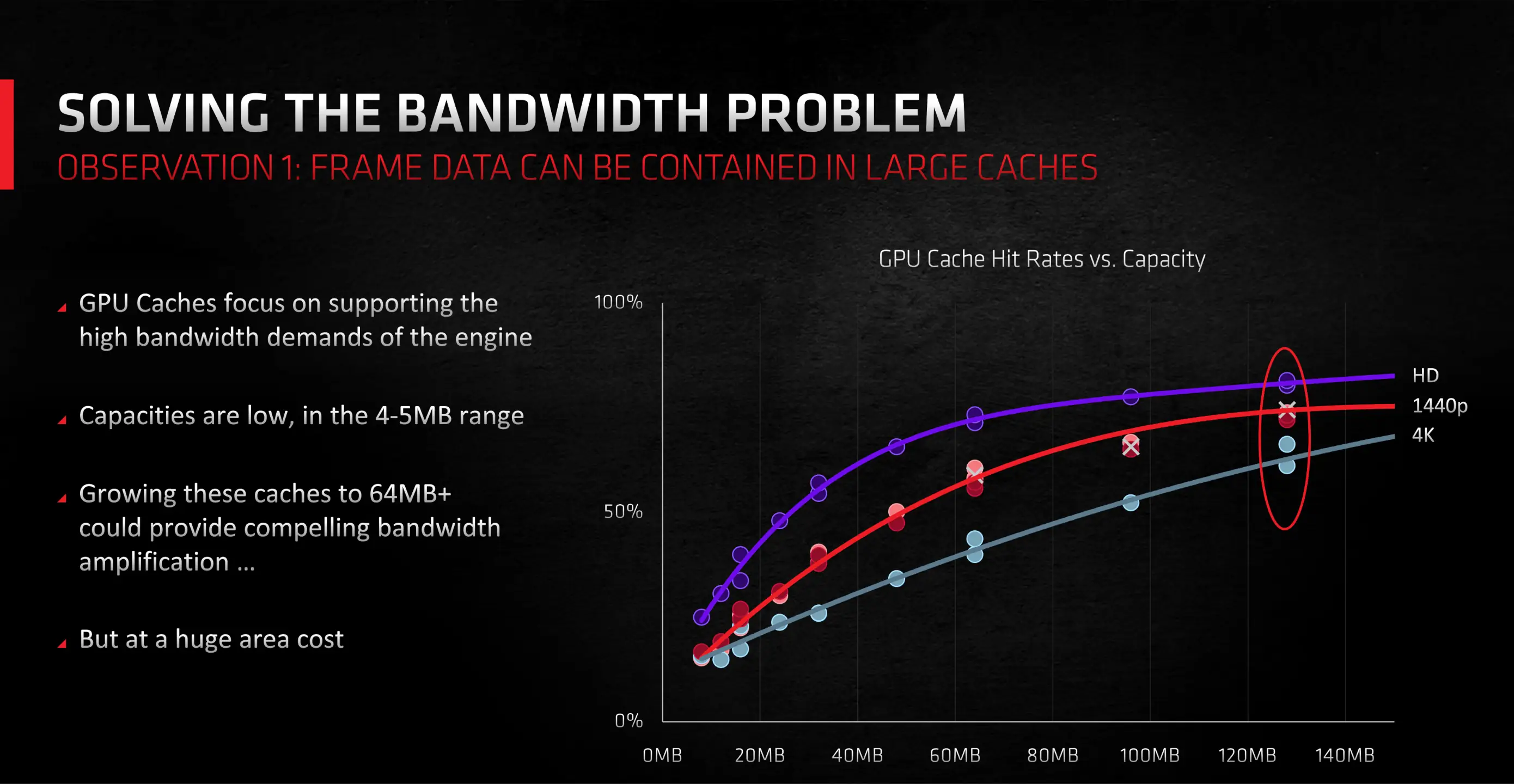
In GPUs, last-level caches are structured such that each VRAM module's interface has its dedicated SRAM slice. The remaining processor utilizes a crossbar connection system to access any module. With GCN and the inaugural RDNA designs, AMD typically employed 256 or 512 kB L3 slices. But with RDNA 2, this surged to an impressive 16 to 32 MB per slice.
This adjustment not only substantially reduced thread delays caused by DRAM reads but also diminished the need for an ultra-wide memory bus. A wider bus necessitates a more expansive GPU die perimeter to accommodate all memory interfaces.
While massive caches can be cumbersome and slow due to inherent long latencies, AMD's design was the opposite – the hulking L3 cache allowed the RDNA 2 chips to have a performance equivalent to that if they had wider memory buses, all while keeping the die sizes under control.
Nvidia followed suit with its latest Ada Lovelace generation and for the same reasons – the previous Ampere design had a maximum L2 cache size of 6 MB in its largest consumer-grade GPU, but this was significantly increased in the new design. The full AD102 die, a cut-down version of which is used in the RTX 4090, contains 96 MB of L2 cache.
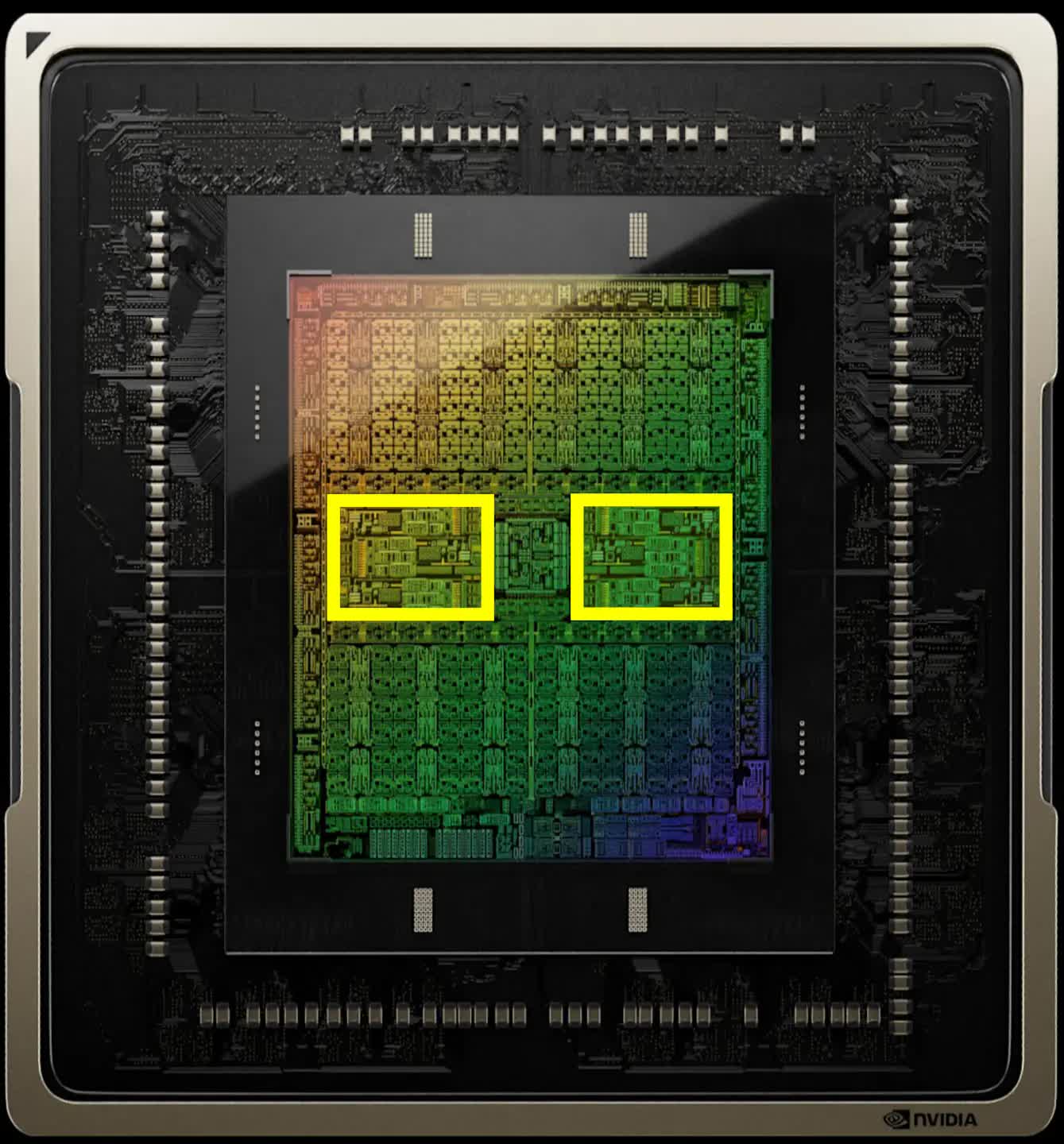
As to why they didn't just go with another level of cache and make that one extremely large, is possibly down to not having the same level of expertise in this area as AMD or perhaps not wanting to seem like it was directly copying the firm. When one looks at the die, shown above, all that L2 cache doesn't actually take up much space on the die, anyway.
In addition to the rise in general-purpose GPU computing, there is another reason why the last-level cache is now so big and it has everything to do with the latest hot topic in rendering: ray tracing.
Big graphics need big data
Without going into too much detail about the process, the act of ray tracing, as used in the latest games, involves carrying out what seems to be a fairly simple algorithm – drawing a line from the position of the camera in the 3D world, through one pixel of the frame, and trace its path through space. When it interacts with an object, check what it is and if it's visible, and from there work out what color to make the pixel.
There's more to it than that, but that's the fundamental process. One aspect of what makes ray tracing so demanding is the object checking. Working out all of the details about the object that the ray has reached is a colossal task, so to help speed up the routine, something called a bounding volume hierarchy is used (BVH for short).
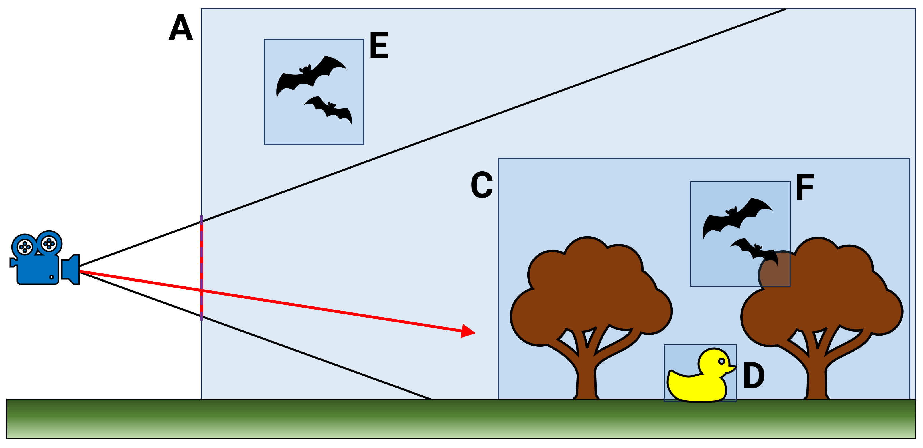
Think of this as being a large database of all the objects that are used within a 3D scene – each entry not only provides information about what the structure is but also how it relates to the other objects. Take the above (and extremely over-simplified) example.
The top of the hierarchy begins with volume A. Everything else is contained within that, but note that volume E is outside of volume C, which itself contains D and F. When a ray is cast out into this scene (the red arrow), a process takes place where the hierarchy is traversed, checking to see what volumes the ray's path passes through.
However, the BVH is arranged like a tree, and the traversal only needs to follow branches where the check results in a hit. So volume E can be rejected immediately, as it's not part of C which the ray will clearly go through. Of course, the reality of a BVH in a modern game is vastly more complex.
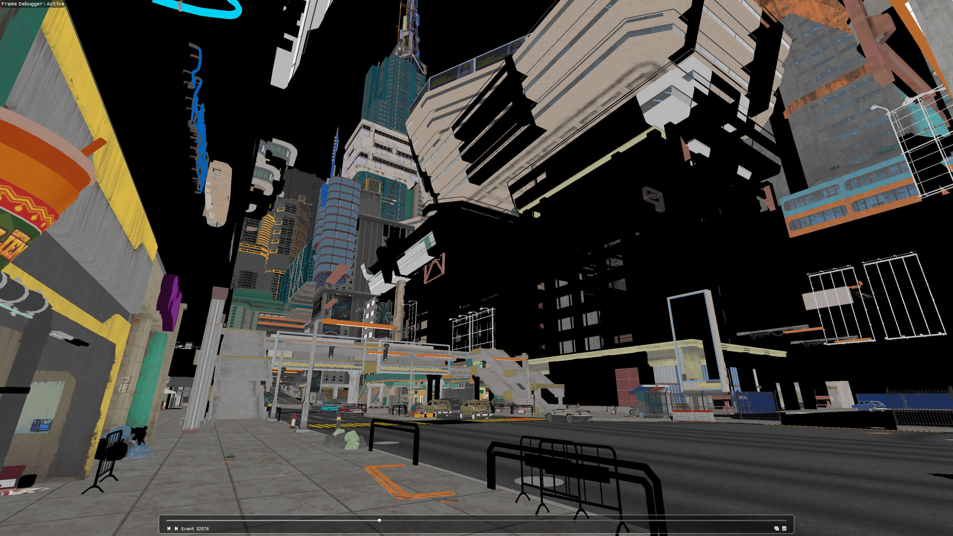
For the above image, we took a snapshot of Cyberpunk 2077, pausing the game's rendering mid-frame to show you how any one given scene is built up through increasing layers of triangles.
Now, try to imagine tracing a line from your eye, through a pixel in the monitor, and then trying to determine exactly which triangle(s) will intersect with the ray. This is why the use of the BVH is so important and it greatly speeds up the whole process.
In this particular game, like many that employ ray tracing to light an entire scene, the BVH comprises multiple databases of two kinds – top-level acceleration structures (TLAS) and bottom-level acceleration structures (BLAS).
The former is essentially a large overview of the entire world, not just the very small part we're looking at. On a PC that uses an Nvidia graphics card, it looks something like this:

We've zoomed in a bit to show you some of the detail it contains, but as you can see, it's verylarge – almost 18 MB in size. Note how the list is one of instances and each one comprises at least one BLAS. The game only uses two TLAS structures (the second is far smaller), but there are many thousands of BLAS in total.
The one below is for an item of clothing that mightbe worn by a character viewed in the world. It might seem like a ridiculous thing to have so many but this hierarchy means if this particular BLAS is not in a larger parent structure that lies in the ray's path, it will never get checked nor used in the coloring stage of the rendering.
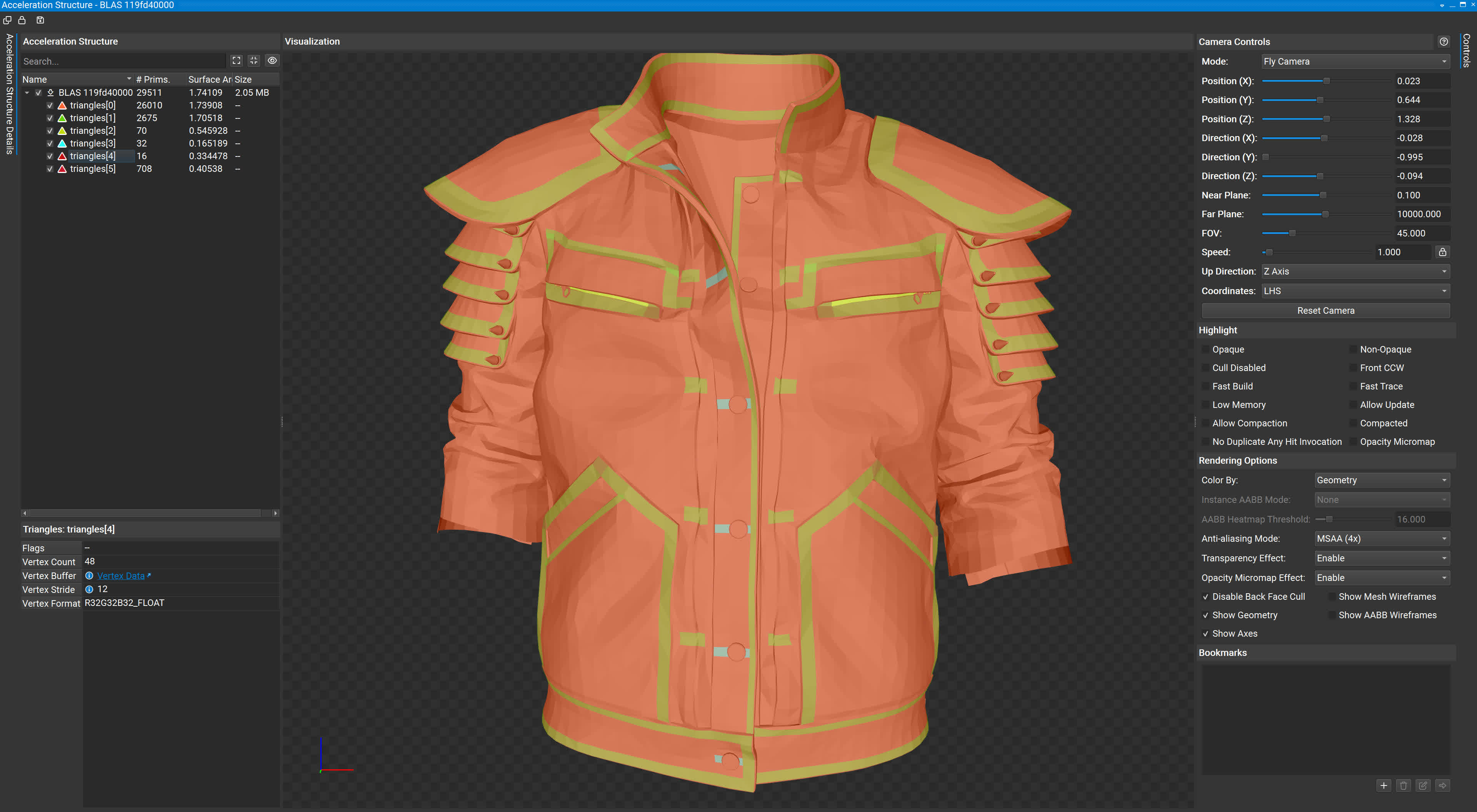
For our snapshot of Cyberpunk 2077, a total of 11,360 BLAS are used, taking up vastly more memory than the TLAS. However, with GPUs now sporting large amounts of cache, there's enough room to store the latter in this SRAM and transfer many of the relevant BLAS across from the VRAM, making the process of ray tracing go much faster.
The so-called holy grail of rendering is still really only accessible to those with the very best graphics cards, and even then, additional technologies (such as image upscaling and frame generation) are employed to bring the overall performance into the realm of playable.
BVHs, thousands of cores, and dedicated ray tracing units in GPUs make all of this possible, but monstrous caches provide a much-needed boost to it all.
Contenders for the crown
Once a few more generations of GPU architectures have passed us by, seeing graphics chips with massive L2 or L3 caches will be the norm, rather than a unique selling point for a new design. GPUs will continue to be used in broad general-purpose scenarios, ray tracing will become increasingly more prevalent in games, and DRAM will still lag behind the developments in processor technologies.
That all said, GPUs won't have it all their way, when it comes to packing in the SRAM. In fact, there are a couple of exceptions to this now.
We're not talking about AMD's X3D range of Ryzen CPUs, even though the Ryzen 9 7950X3D comes with an astonishing 128 MB of L3 cache (Intel's biggest consumer-grade CPU, the Core i9-13900K, gets by with just 36 MB). It's still an AMD product, though, specifically its latest entries in the EPYC 9000 series of server processors.
The $14,756 EPYC 9684X (above) comprises 13 chiplets, twelve of which house the processor's cores and cache. Each of these contains 8 cores and a 64 MB slice of AMD's 3D V-cache on top of the chiplet's built-in 32 MB of L3 cache. Put all together, that's a mind-boggling total of 1152 MB of last-level cache! Even the 16-core version (the 9174F) boasts 256 MB, although it's still not what you'd call cheap, at $3,840.
Of course, such processors aren't designed to be used by mere mortals and their gaming PCs, and the physical size, price tag, and power consumption figure are all so large that we're not going to see anything like them in an ordinary desktop computer for many years.
Part of this is because unlike semiconductor circuitry used for logic units, it's getting increasingly harder to shrink SRAM with each new process node (the method by which chips are manufactured). AMD's EPYC processors have so much cache simply because there are lots of chips underneath the heat spreader.
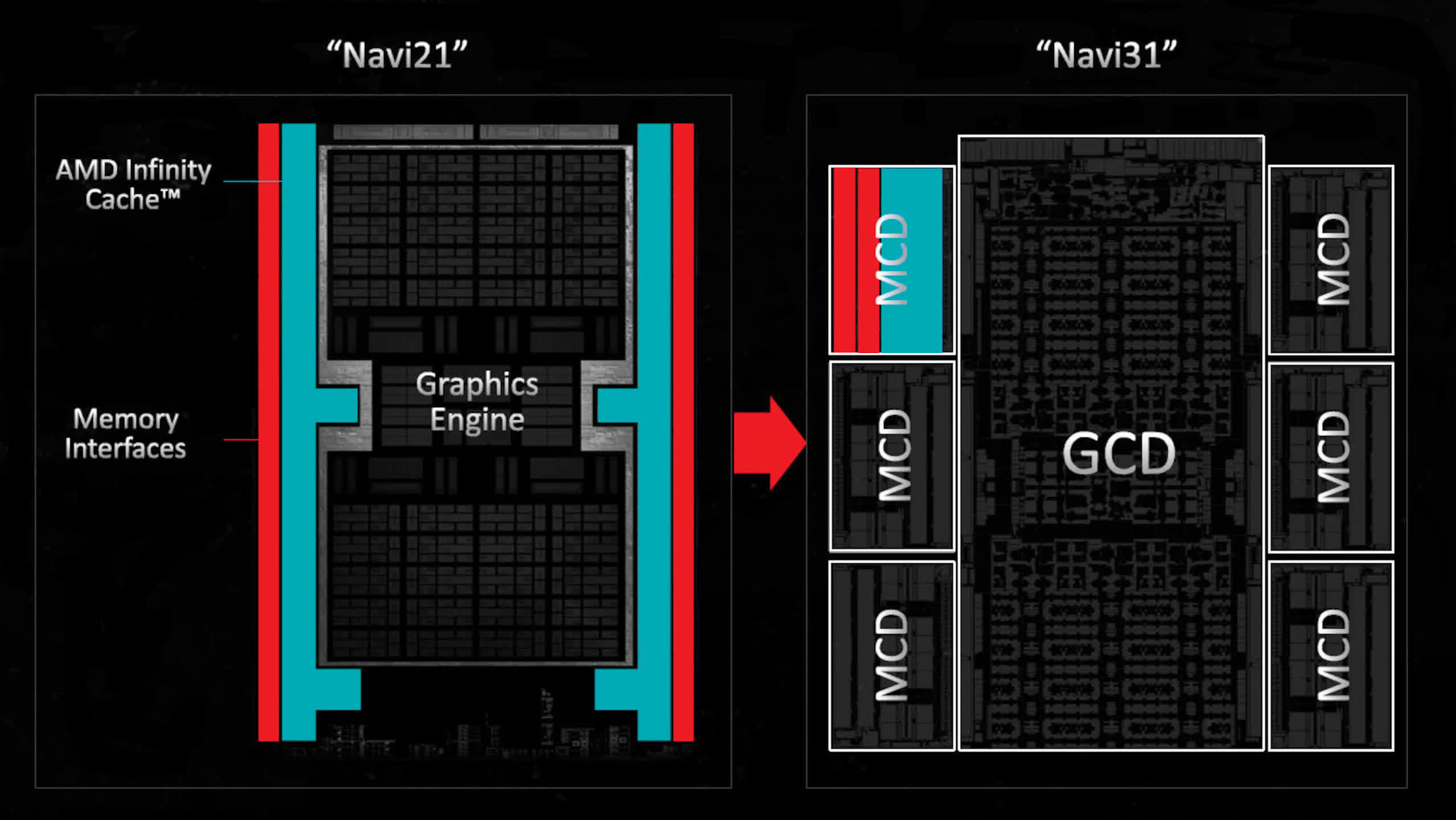
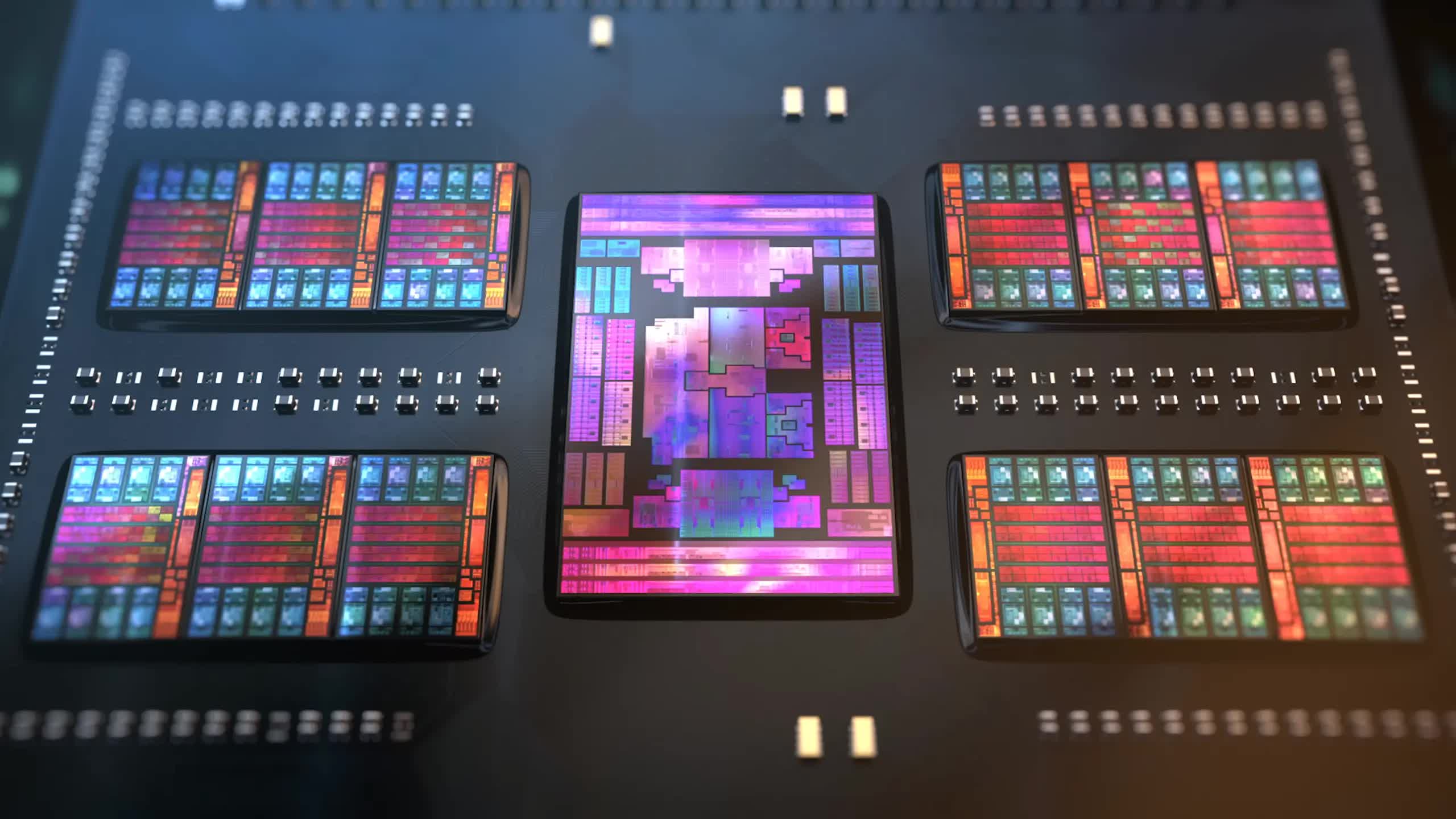
All GPUs will probably go down a similar route at some point in the future and AMD's top-end Radeon 9000 models already do, with the memory interfaces and associated L3 cache slices being housed in separate chiplets to the main processing die.
There are diminishing gains with using ever larger caches though, so don't expect to see GPUs sporting gigabytes worth of cache all over the place. But even so, the recent changes are quite remarkable.
Twenty years ago, graphics chips had very little cache in them, just a handful of kB of SRAM, here and there. Now, you can go out and for less than $400, pick up a graphics card with so much cache, you could fit the entirety of the original Doom inside them – twice over!
GPUs truly are the kings of cache.
Keep Reading. Explainers at TechSpot
- What Are Chiplets and Why They Are So Important for the Future of Processors
- Why Are Modern PC Games Using So Much VRAM?
- Deep Dive: AMD RDNA 3, Intel Arc Alchemist and Nvidia Ada Lovelace GPU Architecture
- Number Representations in Computer Hardware, Explained

Copyright 2022 © coruscomusic.com 泰山压卵网 All Rights Reserved